


1. 寄存器描述
Status Register (SR)
The Status Register is located in the memory map at address 07h. This is a volatile register that provides either control or status of RTC failure, battery mode, alarm trigger, write protection of clock counter, crystal oscillator enable and auto reset of status bits.
状态寄存器(SR)
状态寄存器位于地址07h的内存映射中。这是一个易失性寄存器,提供RTC故障、电池模式、报警触发器、时钟计数器写保护、晶体振荡器启用和状态位自动复位的控制或状态。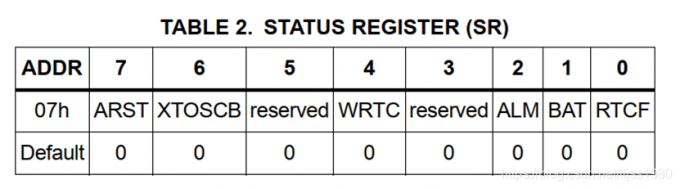
REAL TIME CLOCK FAIL BIT (RTCF)
This bit is set to a “1” after a total power failure. This is a read only bit that is set by hardware (ISL1208 internally) when the device powers up after having lost all power to the device. The bit is set regardless of whether VDD or VBAT is applied first. The loss of only one of the supplies does not set the RTCF bit to “1”. The first valid write to the RTC section after a complete power failure resets the RTCF bit to “0” (writing one byte is sufficient).
实时时钟故障位(RTCF)
完全断电后,该位设置为“1”。这是一个只读位,由硬件(内部为ISL1208)在设备失去所有电源后通电时设置。无论先应用VDD还是VBAT,都会设置该位。只有一个电源丢失不会将RTCF位设置为“1”。完全断电后对RTC部分的第一次有效写入将RTCF位重置为“0”(写入一个字节即可)。
BATTERY BIT (BAT)
This bit is set to a “1” when the device enters battery backup mode. This bit can be reset either manually by the user or automatically reset by enabling the auto-reset bit (see ARST bit). A write to this bit in the SR can only set it to “0”, not “1”.
电池位(BAT)
当设备进入备用电池模式时,该位设置为“1”。该位可以由用户手动复位,也可以通过启用自动复位位自动复位(参见ARST位)。对SR中的该位的写入只能将其设置为“0”,而不是“1”。
ALARM BIT (ALM)
These bits announce if the alarm matches the real time clock. If there is a match, the respective bit is set to “1”. This bit can be manually reset to “0” by the user or automatically reset by enabling the auto-reset bit (see ARST bit). A write to this bit in the SR can only set it to “0”, not “1”. NOTE: An alarm bit that is set by an alarm occurring during an SR read operation will remain set after the read operation is complete.
报警位(ALM)
这些位显示闹钟是否与实时时钟匹配。如果存在匹配,则相应位设置为“1”。该位可由用户手动重置为“0”,或通过启用自动重置位(见ARST位)自动重置。对SR中的该位的写入只能将其设置为“0”,而不是“1”。注:由SR读取操作期间发生的报警设置的报警位将在读取操作完成后保持设置。
WRITE RTC ENABLE BIT (WRTC)
The WRTC bit enables or disables write capability into the RTC Timing Registers. The factory default setting of this bit is “0”. Upon initialization or power up, the WRTC must be set to “1” to enable the RTC. Upon the completion of a valid write (STOP), the RTC starts counting. The RTC internal 1Hz signal is synchronized to the STOP condition during a valid write cycle.
写入RTC启用位(WRTC)
WRTC位启用或禁用RTC定时寄存器的写入功能。此位的出厂默认设置为“0”。初始化或通电时,WRTC必须设置为“1”才能启用RTC。完成有效写入(停止)后,RTC开始计数。RTC内部1Hz信号在有效写入周期内与停止条件同步。
CRYSTAL OSCILLATOR ENABLE BIT (XTOSCB)
This bit enables/disables the internal crystal oscillator. When the XTOSCB is set to “1”, the oscillator is disabled, and the X1 pin allows for an external 32kHz signal to drive the RTC. The XTOSCB bit is set to “0” on powerup.
晶体振荡器使能位(XTOSCB)
此位启用/禁用内部晶体振荡器。当XTOSCB设置为“1”时,振荡器被禁用,X1引脚允许外部32kHz信号驱动RTC。通电时XTOSCB位设置为“0”。
AUTO RESET ENABLE BIT (ARST)
This bit enables/disables the automatic reset of the BAT and ALM status bits only. When ARST bit is set to “1”, these status bits are reset to “0” after a valid read of the respective status register (with a valid STOP condition). When the ARST is cleared to “0”, the user must manually reset the BAT and ALM bits.
自动复位启用位(ARST)
此位仅启用/禁用BAT和ALM状态位的自动复位。当ARST位设置为“1”时,在有效读取相应的状态寄存器(具有有效的停止条件)后,这些状态位被重置为“0”。当ARST清除为“0”时,用户必须手动重置BAT和ALM位。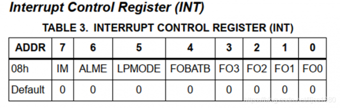
FREQUENCY OUT ConTROL BITS (FO ❤️:0>)
These bits enable/disable the frequency output function and select the output frequency at the IRQ/FOUT pin. See Table 4 for frequency selection. When the frequency mode is enabled, it will override the alarm mode at the IRQ/FOUT pin.
频率输出控制位(FO<3:0>)
这些位启用/禁用频率输出功能,并在IRQ/FOUT引脚选择输出频率。频率选择见表4。启用频率模式时,它将覆盖IRQ/FOUT引脚处的报警模式。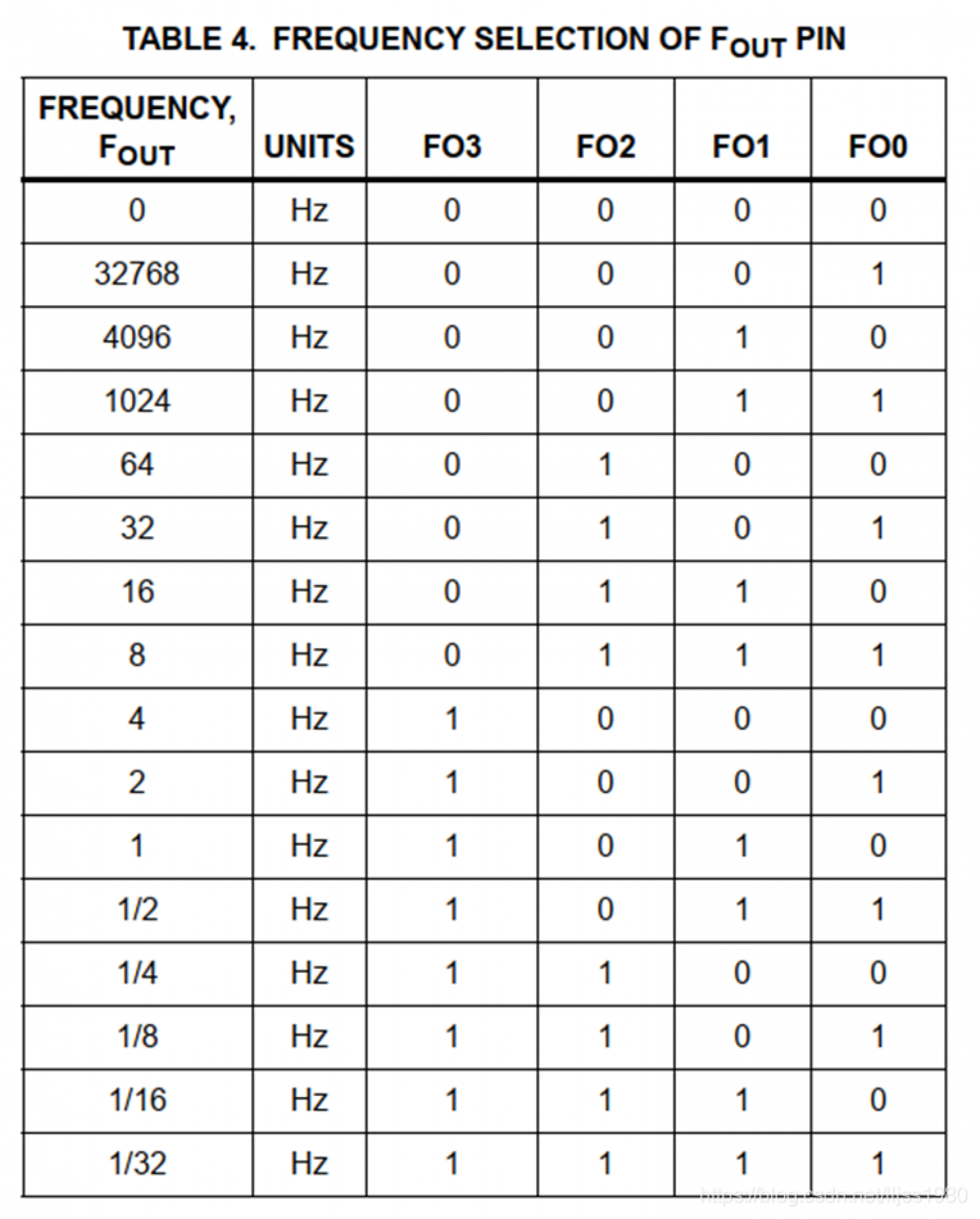
FREQUENCY OUTPUT AND INTERRUPT BIT (FOBATB)
This bit enables/disables the FOUT/IRQ pin during battery backup mode (i.e. VBAT power source active). When the FOBATB is set to “1” the FOUT/IRQ pin is disabled during battery backup mode. This means that both the frequency output and alarm output functions are disabled. When the FOBATB is cleared to “0”, the FOUT/IRQ pin is enabled during battery backup mode.
频率输出和中断位(FOBATB)
此位在电池备份模式(即VBAT电源激活)期间启用/禁用FOUT/IRQ引脚。当FOBATB设置为“1”时,FOUT/IRQ引脚在电池备用模式下被禁用。这意味着频率输出和报警输出功能都被禁用。当FOBATB清除为“0”时,FOUT/IRQ引脚在电池备用模式下启用。
LOW POWER MODE BIT (LPMODE)
This bit enables/disables low power mode. With LPMODE = “0”, the device will be in normal mode and the VBAT supply will be used when VDD < VBAT – VBATHYS and VDD < VTRIP. With LPMODE = “1”, the device will be in low power mode and the VBAT supply will be used when VDD < VBAT – VBATHYS. There is a supply current saving of about 600nA when using LPMODE = “1” with VDD = 5V. (See Typical Performance Curves: IDD vs VCC with LPMODE ON & OFF.)
低功耗模式位(LPMODE)
此位启用/禁用低功率模式。当LPMODE=“0”时,设备将处于正常模式,当VDD<VBAT-VBATHYS和VDD<VTRIP时,将使用VBAT电源。当LPMODE=“1”时,设备将处于低功率模式,当VDD<VBAT-VBATHYS时,将使用VBAT电源。当使用LPMODE=“1”和VDD=5V时,可节省约600nA的电源电流(见典型性能曲线:LPMODE打开和关闭时的IDD与VCC)
ALARM ENABLE BIT (ALME)
This bit enables/disables the alarm function. When the ALME bit is set to “1”, the alarm function is enabled. When the ALME is cleared to “0”, the alarm function is disabled. The alarm function can operate in either a single event alarm or a periodic interrupt alarm (see IM bit). NOTE: When the frequency output mode is enabled, the alarm function is disabled.